24-hour hotline:+8613662168047
Keyword search: battery plant , lithium battery factory , power bank works , lifepo4 battery mill , Pallet Trucks LiFePO4 Battery, LiFePO4 Pallet Trucks Battery, Lithium Pallet Trucks Battery,
Introduction to Silicon Solar Cells
Si silicon, atomic number 14, atomic weight 28.0855, has two forms: crystalline and amorphous. Solar energy is an inexhaustible renewable energy source for humanity. It is also a clean energy source that does not produce any environmental pollution.
In the effective utilization of solar energy; Solar photovoltaic utilization is the fastest developing and most dynamic research field in recent years, and is one of the most eye-catching projects.
Classification of silicon solar cells
The production of solar cells is mainly based on semiconductor materials, and its working principle is to use photoelectric materials to absorb light energy and undergo photoelectric conversion reactions. According to the different materials used, solar cells can be divided into:
1. Silicon solar cells;
2. Batteries made from inorganic salts such as gallium arsenide III-V compounds, cadmium sulfide, copper indium selenium, and other multi-component compounds;
3. Solar cells prepared from functional polymer materials;
4. Nanocrystalline solar cells, etc.
1、 Silicon solar cells
1. Working principle and structure of silicon solar cells
The principle of solar cell power generation is mainly the photoelectric effect of semiconductors, and the general structure of semiconductors is as follows:
Silicon material is a semiconductor material, and the principle of solar cell power generation mainly utilizes the photoelectric effect of this semiconductor. The molecular structure of a typical semiconductor is as follows:
A positive charge represents a silicon atom, while a negative charge represents the four electrons surrounding the silicon atom.
When other impurities are added to silicon crystals, such as boron (black or silver gray solid, melting point 2300 ℃, boiling point 3658 ℃, density 2.34 g/cm, hardness second only to diamond, stable at room temperature, can react with nitrogen, carbon, and silicon. At high temperatures, boron also reacts with many metals and metal oxides to form metal borides. These compounds are usually high hardness, melting resistance, high conductivity, and chemically inert substances.) Phosphorus, etc. When boron is added, there will be a hole in the silicon crystal, and its formation can be explained by referring to the following figure:
A positive charge represents a silicon atom, a negative charge represents the four electrons surrounding the silicon atom, and a yellow charge represents the doped boron atom. Since there are only three electrons around the boron atom, a blue hole is generated as shown in the figure. This hole becomes unstable due to the lack of electrons, easily absorbing electrons and neutralizing them, forming a P (positive) type semiconductor.
(Attached, what is a P-type semiconductor? Adding trivalent element impurities to semiconductor materials such as silicon or germanium crystals can form a P-type semiconductor with missing shell particles, while adding pentavalent element impurities can form an N-type semiconductor with excess shell particles.)
Similarly, after doping with phosphorus atoms, because phosphorus atoms have five electrons, one electron becomes very active, forming an N (negative) type semiconductor. The yellow ones represent phosphorus nuclei, and the red ones represent excess electrons,
P-type semiconductors contain more holes, while N-type semiconductors contain more electrons. Therefore, when P-type and N-type semiconductors combine, a potential difference will be formed at the contact surface, which is the PN junction.
When P-type and N-type semiconductors are combined, a special thin layer is formed in the interface area between the two semiconductors. The P-type side of the interface is negatively charged, while the N-type side is positively charged. This is due to the presence of multiple holes in P-type semiconductors and multiple free electrons in N-type semiconductors, resulting in a concentration difference. The holes in the P region will spontaneously diffuse to the N region, and the electrons in the N region will spontaneously diffuse to the P region. Due to the orientation of electrons and holes, P-type semiconductors that were originally electrically neutral will accumulate negative charges near the interface (due to some holes diffusing to the N region). Similarly, N-type semiconductors that were originally electrically neutral will accumulate positive charges near the interface (due to some electrons diffusing to the P region), forming an "internal electric field" with N pointing towards P, thereby preventing the diffusion of electrons and holes. After reaching equilibrium, a special thin layer is formed to form a potential difference, thus forming a PN junction. When the chip is exposed to light, the holes in the N-type semiconductor move towards the P-type region in the PN junction, and the electrons in the P-type region move towards the N-type region, forming a current from the N-type region to the P-type region. Then, a potential difference is formed in the PN junction, which forms the power source. Here is the power diagram.
Due to the fact that semiconductors are not good conductors of electricity, if electrons flow through the p-n junction in the semiconductor, the resistance is very high and the loss is also very high. But if all the metal is coated on the upper layer, sunlight cannot pass through and current cannot be generated. Therefore, a metal mesh is generally used to cover the p-n junction (as shown in the comb shaped electrode) to increase the area of incident light.
In addition, the surface of silicon is very bright and will reflect a large amount of sunlight, which cannot be utilized by batteries. For this reason, scientists coated it with a protective film with a very low reflection coefficient. In actual industrial production, a layer of silicon nitride film is usually deposited by chemical vapor deposition, with a thickness of about 1000 angstroms. Reduce reflection loss to 5% or even less. The current and voltage that a battery can provide are limited, so many batteries (usually 36) are connected in parallel or series to form solar photovoltaic panels.
2. Production process of silicon solar cells
The typical crystalline silicon solar cells are available in thicknesses of 350-450 μ Made from high-quality silicon wafers, this type of silicon wafer is sawn and cut from silicon ingots that are pulled or cast.
The above method actually consumes more silicon material. In order to save materials, chemical vapor deposition (CVD) is commonly used to prepare polycrystalline silicon thin film batteries, including low-pressure chemical vapor deposition (LPCVD) and plasma enhanced chemical vapor deposition (PECVD) processes. In addition, liquid phase epitaxy (LPPE) and sputtering deposition methods can also be used to prepare polycrystalline silicon thin film batteries.
2、 Nanocrystalline chemical solar cells
Silicon solar cells are undoubtedly the most mature among solar cells, but due to their high cost, they cannot meet the requirements for large-scale promotion and application. For this reason, people have been constantly exploring processes, new materials, and thin-film solar cells, among which the recently developed nano TiO2 crystal chemical energy solar cells have received attention from scientists at home and abroad.
Taking dye sensitized nanocrystalline solar cells (DSSCs) as an example, these cells mainly include a glass substrate coated with a transparent conductive film, dye sensitized semiconductor materials, counter electrodes, and electrolytes.
Anode: Dye sensitized semiconductor thin film (TiO2 film)
Cathode: Platinum plated conductive glass
Electrolyte: I3/I
As shown in the figure, the white ball represents TiO2, and the red ball represents dye molecules. Dye molecules absorb solar energy and transition to excited states, which are unstable. Electrons quickly inject into the adjacent TiO2 conduction band, and the electrons lost in the dye are quickly compensated from the electrolyte. The electricity entering the TiO2 conduction band eventually enters the conductive film, and then generates photocurrent through an external circuit.
The advantages of nanocrystalline TiO2 solar cells lie in their low cost, simple process, and stable performance. Its photoelectric efficiency is stable at over 10%, and the production cost is only 1/5 to 1/10 of that of silicon solar cells. Its lifespan can reach over 20 years. However, as the research and development of such batteries have just begun, it is estimated that they will gradually enter the market in the near future.
3、 Handmade production of dye sensitized TiO2 solar cells
1. Production of titanium dioxide film
(1) First, put the titanium dioxide powder into a mortar and grind it with the adhesive
(2) Then slowly coat the conductive glass with a glass rod
(3) Sinter the titanium dioxide film under an alcohol lamp for 10-15 minutes, then cool it down
2. Use natural dyes to color titanium dioxide
Add one tablespoon of fresh or frozen black plums, mountain plums, pomegranate seeds, or black tea to water and squeeze, then put in a titanium dioxide film for coloring, which takes about 5 minutes until the film layer turns dark purple. If the coloring on both sides of the film layer is uneven, soak it in water for another 5 minutes, then rinse with ethanol and gently dry with soft paper.
3. Making positive electrodes
TiO2, colored by dyes, serves as the electrode (i.e. negative electrode) where electrons flow out. The positive electrode can be composed of a conductive surface of conductive glass (coated with a conductive SnO2 film layer). A simple multimeter can be used to determine which side of the glass is conductive, and fingers can also be used to make judgments. The conductive surface is relatively rough. As shown in the figure, mark the non-conductive surface with a "+" and then evenly apply a layer of graphite on the conductive surface with a pencil.
4. Add electrolyte
Using a solution containing iodine ions as the electrolyte for solar cells, it is mainly used for reducing and regenerating dyes. As shown in the figure, one to two drops of electrolyte can be added to the surface of the titanium dioxide film.
5. Assemble the battery
Place the colored titanium dioxide film facing up on a table, drop one to two drops of electrolyte containing iodine and iodine ions on the film, and then press the conductive surface of the positive electrode facing down on the titanium dioxide film. Slightly stagger the two pieces of glass and use two clips to clamp the battery. The exposed parts of the two pieces of glass are used to connect the wires. In this way, your solar cell is made.
6. Battery testing
Check if your solar cell can generate current under outdoor sunlight.
structure
A positive charge represents a silicon atom, while a negative charge represents the four electrons surrounding the silicon atom.
When other impurities such as boron and phosphorus are added to the silicon crystal, a hole will exist in the silicon crystal. Its formation can be seen in the following figure:
A positive charge represents a silicon atom, while a negative charge represents the four electrons surrounding the silicon atom. The yellow one represents the doped boron atom, as there are only three electrons around the boron atom, blue holes will be generated.
When P-type and N-type semiconductors are combined, a special thin layer is formed in the interface area between the two semiconductors. Electrons from the N region will diffuse to the P region, while holes from the P region will diffuse to the N region. Once diffused, an internal electric field from N to P is formed, thereby preventing diffusion. Until equilibrium is reached, a special thin layer is formed to form a potential difference, which is the PN junction.
Due to the fact that semiconductors are not good conductors of electricity, electrons flow through the p-n junction in the semiconductor. Therefore, a metal mesh is generally used to cover the p-n junction (as shown in the comb shaped electrode) to increase the area of incident light.
In addition, the surface of silicon is very bright and reflects a large amount of sunlight, which cannot be utilized by batteries. Scientists have coated it with a protective film with a very low reflection coefficient.
Working principle of silicon solar cells
A solar cell is a device that responds to light and can convert light energy into electricity. There are many types of materials that can generate photovoltaic effects, such as monocrystalline silicon, polycrystalline silicon, amorphous silicon, gallium arsenide, selenium indium copper, etc. Their power generation principles are basically the same, and now we will take crystalline silicon as an example to describe the process of photovoltaic power generation. P-type crystalline silicon can be doped with phosphorus to obtain N-type silicon, forming a P-N junction.
When light shines on the surface of a solar cell, a portion of the photons are absorbed by the silicon material; The energy of photons is transferred to silicon atoms, causing electrons to transition and become free electrons. They gather on both sides of the P-N junction, forming a potential difference. When an external circuit is connected, under the action of this voltage, a current will flow through the external circuit to generate a certain output power. The essence of this process is the conversion of photon energy into electrical energy.
production process
Chemical vapor deposition mainly uses SiH2Cl2, SiHCl3, SiCl4 or SiH4 as reaction gases, which react under a certain protective atmosphere to generate silicon atoms and deposit them on a heated substrate. The substrate materials generally include Si, SiO2, Si3N4, etc. But research has found that it is difficult to form larger grains on non silicon substrates and it is easy to form voids between grains. The solution to this problem is to first deposit a thin layer of amorphous silicon on the substrate using LPCVD, then anneal this layer of amorphous silicon to obtain larger grains, and then deposit a thick polycrystalline silicon film on this layer of seed crystals. Therefore, recrystallization technology is undoubtedly an important link, and the main technologies used include solid-state crystallization and intermediate zone melting recrystallization. In addition to using recrystallization technology, polycrystalline silicon thin film solar cells also use almost all techniques for preparing monocrystalline silicon solar cells, which significantly improves the conversion efficiency of the solar cells produced.

Lithium Batteries ,Ensure Quality
Our lithium battery production line has a complete and scientific quality management system
Ensure the product quality of lithium batteries
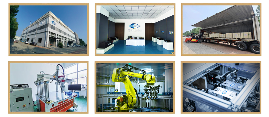
Years of experience in producing lithium batteries
Focus on the production of lithium batteries
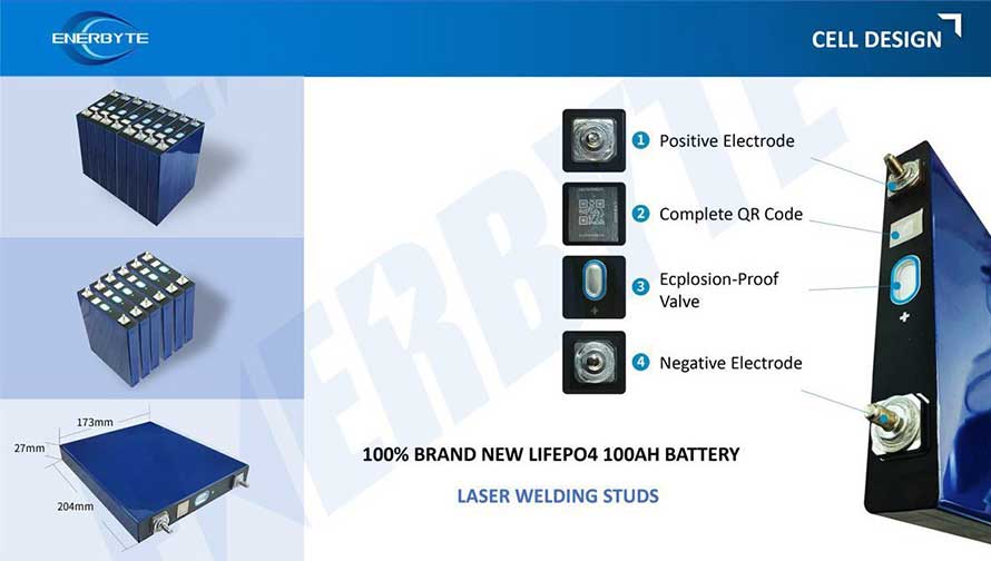
WE PROMISE TO MAKE EVERY LITHIUM BATTERY WELL
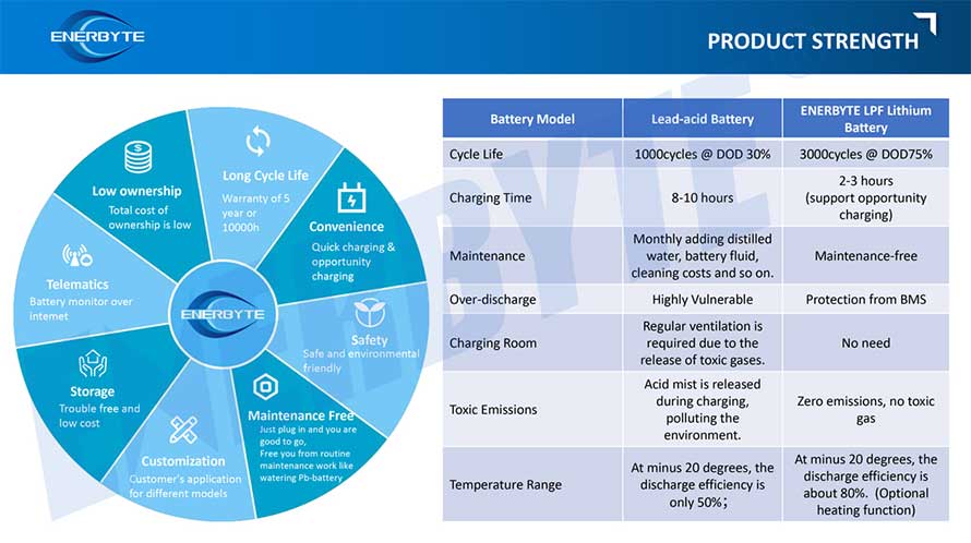
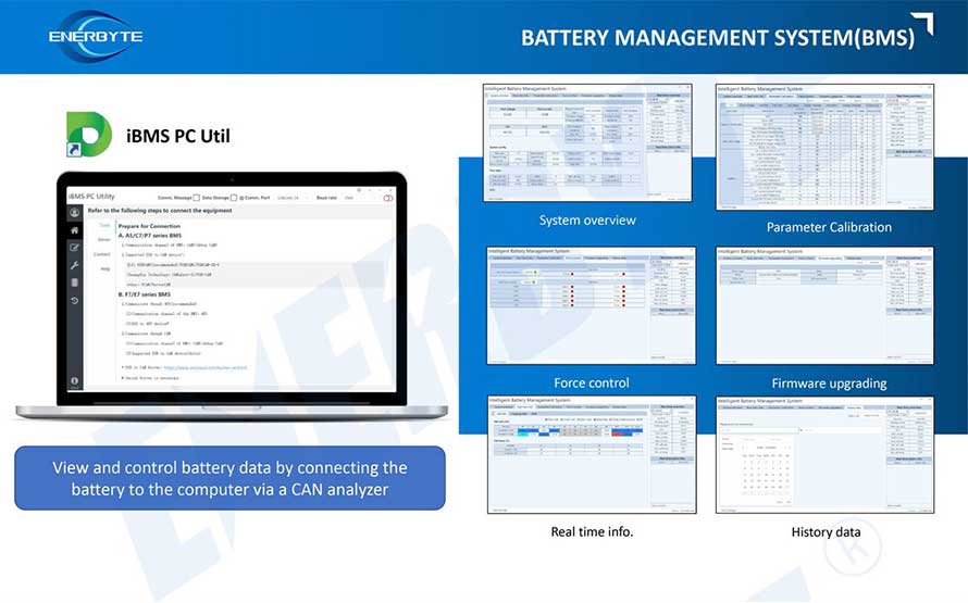
We have a comprehensive explanation of lithium batteries
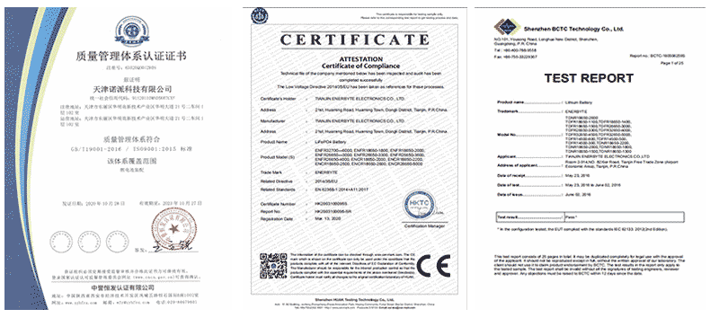
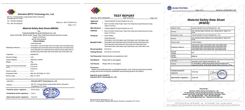
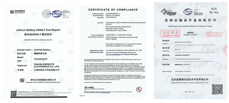
QUALIFICATION CERTIFICATE
THE QUALITY OF COMPLIANCE PROVIDES GUARANTEE FOR CUSTOMERS
MULTIPLE QUALIFICATION CERTIFICATES TO ENSURE STABLE PRODUCT QUALITY
Providing customers with professional and assured products is the guarantee of our continuous progress.

Applicable brands of our products


 Service hotline